Boost Safety
Boost Safety
Reduce worker exposure to light and chemicals.
Enhance Efficiency
Enhance Efficiency
Increase wafer defect detection accuracy.
Cut Costs
Cut Costs
Reduce staffing and inspection expenditures.
Overview
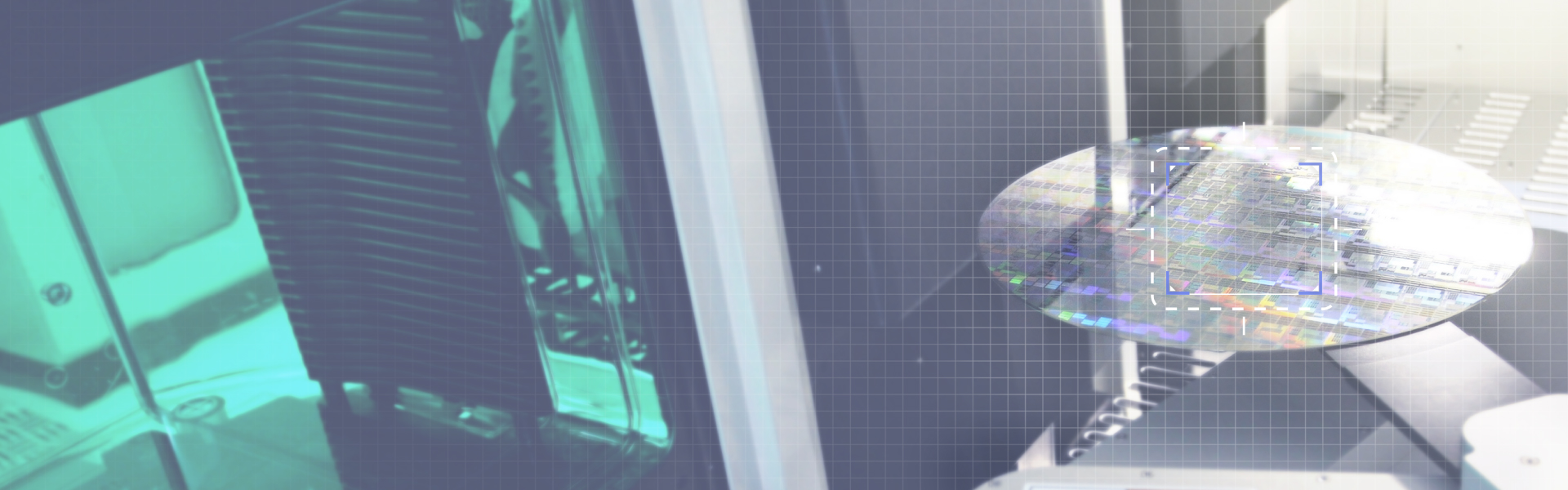
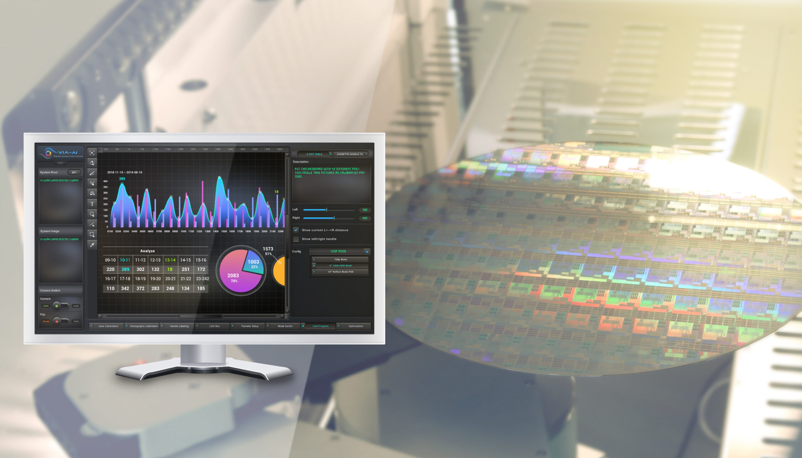
Accelerate the detection of defective wafers using our high-precision visual inspection solution.
Running an optimized AI model that identifies defects by analyzing wafer images taken by an industrial camera, this cutting-edge solution is suitable for use on all sizes of wafer. By eliminating human errors resulting from inattentiveness, fatigue, and poor judgment, our wafer inspection solution delivers pinpoint levels of accuracy in identifying even the slightest defects, achieving a recall rate of nearly 100% and a false positive rate of less than 5%.
By automating the inspection process, the solution enables silicon wafer manufacturers and assembly houses to accomplish significant gains in plant efficiency and operator safety. With its powerful Edge AI processing capabilities and seamless connectivity to an ERP network or corporate cloud, the solution also provides a wealth of data analysis and insights that enterprises can harness to further boost operational efficiency and safety.
Features
The wafer visual inspection solution is fast and easy to deploy and is scalable across multiple production lines. The solution is comprised of the following key components and can be customized to meet specific usage requirements:
AI inferencing and training server
Dedicated wafer defect detection AI model
USB industrial camera
Use Cases
The wafer visual inspection solution has enabled one of the world’s leading semiconductor companies to speed up the defect detection process, reduce staffing costs, and create a safer and cleaner environment.
Get In Touch
Maximize wafer production quality with the state-of-the-art VIA Wafer Inspection Solution, providing precise inspection capabilities, minimizing defects, and optimizing manufacturing efficiency. Contact us for more information!